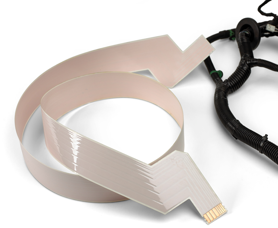
Specialty Circuits
The Design is More Than Half the Battle
Thanks to a completely tool-less manufacturing process, CelLink’s
minimum order quantity is one.
The Design is More Than Half the Battle
Thanks to a completely tool-less manufacturing process, CelLink’s
minimum order quantity is one.

CelLink’s tool-less, lamination-based manufacturing technology allows for the rapid prototyping of new designs with short lead times. Once a design is fully optimized, the exact same process is used to produce circuits at high volume and low cost, simplifying the path from prototype to production.
CelLink has the ability to incorporate a wide variety of metals and insulators into its circuits; essentially any material that can be provided as a foil or thermally-activated film can be processed. With the ability to produce patterned metal layers as thick as 500 µm, CelLink bridges the capability gap between etched PCBs and stamped busbars.
CelLink’s process is highly conducive to producing two-side exposed metal features such as back-bared structures, free standing fuses, and exposed leads. These features can be produced with a much simpler process and at a lower price point than traditional flex.
Through careful control of manufacturing tolerances and optimization of materials, CelLink can achieve a pattern accuracy of 0.01% on large parts – that’s 100 µm per meter.
Have a thick-metal, large-area, or otherwise unique design that can’t be produced elsewhere? Contact us!